The application of 3D printing technology in PCBA manufacturing is revolutionizing traditional production workflows, offering unprecedented design flexibility, rapid prototyping capabilities, and cost savings for both small-batch customization and large-scale production. Unlike conventional subtractive manufacturing methods (e.g., CNC milling and etching) that generate significant material waste, 3D printing (additive manufacturing) builds PCBA layer by layer using conductive and dielectric materials, enabling the realization of complex geometries that are impossible or cost-prohibitive with traditional techniques. This technology has been widely adopted in industries such as aerospace, medical devices, IoT, and consumer electronics, where personalized designs and rapid time-to-market are critical.
Key applications of 3D printing in PCBA include rapid prototyping, complex structure fabrication, and recyclable circuit assembly. In prototyping, 3D printing reduces the development cycle from 14-21 days (traditional process) to 24-72 hours, allowing engineers to iterate designs quickly and validate concepts in less than 48 hours. For example, DissolvPCB, a 3D-printed PCBA technology using polyvinyl alcohol (PVA) as a water-soluble substrate and eutectic gallium-indium (EGaIn) as conductive material, enables full recyclability—obsolete PCBA can be dissolved in water to recover components and reusable materials, addressing the growing e-waste problem. In complex structure fabrication, 3D printing supports conformal printing on non-planar surfaces, curved PCBs for wearable devices (radius < 5mm), and embedded passive components, reducing the size and weight of electronic devices while improving performance. Aerosol jet printing, a type of 3D printing, can print nano-metallic inks (Ag, Cu, Ni) with line width control of 10-100μm at 50 mm/s, making it suitable for high-density interconnect (HDI) PCBA in 5G and AI devices.
Moreover, 3D printing enables the integration of multi-material and multi-functional PCBA in a single fabrication step. Dual-extrusion 3D printers can simultaneously deposit dielectric and conductive materials, while hybrid systems combine copper-filled thermoplastics with laser-activated conductive pathways, enhancing the versatility of PCBA designs. Industry case studies show that 3D-printed PCBA achieves 98.7% electrical connectivity, with applications ranging from Bluetooth speakers and fidget toys to aerospace sensors. As 3D printing materials (e.g., conductive polymers, nanoparticle inks) and processes continue to advance, the technology is expected to replace traditional manufacturing for more complex PCBA applications, driving innovation in electronic device design and production efficiency.
Read recommendations:
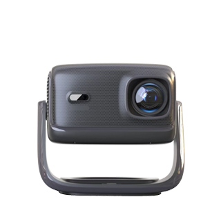
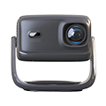
HN30B Portable - HN Series Projector
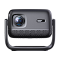
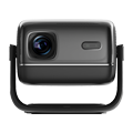
250 ANSI Lumens 1080P Home Theater Projector
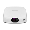
3d Projector for office meeting room


 Reviewed: